| Print, video, sounds |
|
1. Overview 51.1 Thermal Issues in Integrated Circuits. 51.2 Thermal performance of integrated circuits. 5 1.3 Ambient verses die temperature. 6 1.4 Die temperature. 7 1.5 It's all about the die temperature. 8 1.6 Conclusion. 9 2. ESD Diode temp measurement 102.1 Theory. 102.2 Practice. 12 2.2.1 The part my be self heating 12 2.2.2 Oven set point temp may be inaccurate 12 2.2.3 The diode currents may be different 12 2.2.4 external circuitry distorts the measurement. 13 2.2.5 internal circuitry distorts the measurement. 13 2.2.6 The test equipment may induce errors. 13 2.2.7 power distort the measurement. 13 2.3 Procedure. 14 2.3.1 Pick the pin(s). 14 2.3.2 Prepare the board. 15 2.3.3 Calibrate the ESD diodes in an oven. 15 2.3.4 internal resistance correction factor. 16 2.3.5 corrected ESD diode voltage 18 |
 |
  |
3. Thermal Camera temp measure 193.1 Theory. 193.2 Practice. 19 3.2.1 The emissivity of the hot surface. 19 3.2.2 The focusing of the camera. 20 3.2.3 software parameters on the measurement. 20 3.2.4 A calibration method. 21 3.3 Procedure. 22 3.3.1 De-cap the parts and mount on the board. 22 3.3.2 Paint the chip die flat black. 23 3.3.3 Place the board under the camera, focus. 23 3.3.4 Proper correction factors in the software. 24 3.3.5 Take the scan and adjust the colormap. 25 4. Conclusions and Recommendations 274.1 measure ESD diode temp as part operates. 274.2 Significant thermal gradients across the die. 27 4.3 Further investigations are needed 27 5. Action Plan 285.1 ESD Diode Method. 285.1.1 instantaneous change calculating IR drop. 28 5.1.2 bondwires & Vcc plane resistance directly 28 5.1.3 CAD/SPICE methods for sheet resistivity. 28 5.2 Thermal camera method. 28 5.2.1 Create a calibration circuit. 28 5.2.2 Investigate high resolution imagers. 28 5.2.3 Investigate stronger lenses. 28 |
 |
  |
|
Semiconductor physics is not kind at cold temperatures either. The betas of the transistors go down, the Gm goes up and the Vbe voltage goes up. All this can cause instabilities and non-functionality in a part. At least these problems will go away when the part gets warmer. This paper is more concerned with the measurement of excessive temperatures at the die. 1.2 Thermal performance of ICs. Analog engineers (perhaps I should simply say "real" engineers) intuitively understand that any circuit will change operation with temperature. This is true for the components on the circuit board as well as the components integrated inside any IC. It is a relatively straightforward matter to put a board or IC into an oven and measure it's performance change over temperature. Most IC datasheets have at least one chart that relates some parameter to temperature. What seems to be far less understood is the relationship to temperature if the part under question is making it's own power. Power supply chip users are more familiar then most other engineers with this issue. It must be understood that the concept of ambient (room) temperature and the IC temperature are two different things. It the part is a CMOS op amp that is driving a very high resistance load it is a safe bet that the part itself is not heating up due to power dissipation. If you put it in a 150°C oven the silicon die inside the part will be at 150°C with perhaps a few tenths of a degree more due to the power being lost inside the die. Things are very different with an IC that is delivering appreciable power. The die temperature is raised by the power being dissipated by the output transistors. For high-speed bipolar parts the quiescent current of the part may also contribute to the heating. The power due to quiescent heating is simple to figure. It is the |
 |
  |
|
current into the part times the voltage across the part. The power being dissipated by the output transistors is a little more difficult. It is not necessarily proportional to current. This is because the power in the output transistors is the current trough the transistor times the voltage across the transistor. This means that a part may be putting a lot of power into a load but the output transistor is fully saturated. All that it is doing is connecting the load to the power supply and there is less then a volt across the transistor. If the part is putting 100 mA out the power is maybe 0.5 volts times 100 mA for a power of 0.05 Watts being dissipated in the output transistor. Now change the load from a nice large value resistor to a diode connected to ground. The diode means that the output can never get much above 0.6 volts. If the amplifier is putting out the same 100 mA and if it is powered of 12 volts that means the power being dissipated is 100mA times 11.4 volts or 1.14 Watts. That is a lot of power and there better be good heat sinking on the part and the part package better be able to handle these power levels. 1.3 Ambient verses die temperature. When the part is dissipating it's own power the relation ship between ambient and die temperature is no longer so simple. If the part is dissipating a watt and you put it in an oven at 150 °C it is guaranteed that the die will be significantly above 150°C. Even if you calculate the exact power being dissipated in the part (i.e., you know the exact load and operating conditions) this still is not enough to know how much higher the die temperature will be to the oven temperature. This is because the resultant temperature of the die is dependent on the heat sinking and package that the part is mounted in. This should be intuitive with a little thought. If the part was wired up with really thin wires so very little heat can conduct out of the part from the connections, and you |
 |
  |
|
wrapped the part up in Styrofoam insulation it is guaranteed you will melt the part when you try to make it dissipate 1 watt internally. The temperature has to go way up because the heat is trapped and can not flow anywhere. If you throw that same die into a bath of florinert liquid the heat can now transfer to the liquid. Since it will transfer by fluid convection, this is a very efficient transfer--the florinert that gets hot rises up and the die gets constantly bathed with cool florinert. Although there are web sites that try to immerse an entire computer in $800 a gallon florinert it is generally impractical. A real system will have a part mounted on a conventional FR4 (green fiberglass) circuit board. The heat can then get out of the part in several ways. Most of it is conducted out of the part by the copper traces on the circuit board. If the part has a die attach paddle like our LLP parts this can be very efficient. A smaller amount of heat is also convected to the air directly from the part. A heat sink can be mounted on top of the part but if it only touches the plastic this is not very efficient since the thermal conductivity of plastic is so much worse then metal. For instance the plastic has a 0.837 w/m.C thermal conductivity and copper has 377 w/m.c thermal conductivity. This means copper is 450 times more thermally conductive then plastic. Once the heat gets out to the circuit traces and planes the same issue still applies--if you wrap the entire board in Styrofoam to keep the heat from going anywhere else the part will still melt, it will only take a little longer since it gets to heat up the circuit board too. What usually happens is that the circuit board transfers the heat to the air. You can think of the circuit board (and any heat sinks) as a heat spreader that allows the heat to come in contact with a large surface area of air. Since heat transfer to air is convective it has the same benefit as florinert, the hot air rises away from the board and the cool air constantly replenishes the area around the |
 |
  |
|
board. If you want to improve the situation you can blow the hot air off the board with a fan. One little understood fact is that as you increase in altitude the air gets thinner and the convective cooling is substantially reduces. There is a small but noticeable effect when you are in Denver. In a jet fighter at 70,000 feet there is essentially no convective cooling. Electronics designed for these systems must carry all the heat away conductively, though metal plates touching all the parts to clamps on the sides of the board and then down to a liquid cooled cold-plate. The ambient temperature in this case is irrelevant to the die temperature. 1.4 Die temperature. What really matters to IC performance is what temperature the die is. That is not to say that a temperature change on the load may change its characteristics and cause performance issues. Still, when we measure and characterize ICs all we can know is what temperature the die is at. A real world application needs to characterize both the load and operating conditions (mostly supply voltage) as well as the thermal capabilities of the package and circuit board as well as the thermal environment. Just because the data-sheet says the part can operate over a -40 to +85°C ambient does not mean the part will not burn up if you do not limit the power being dissipated in the IC as well as provide a good thermal path for the power that is dissipated to leave the die (figure 1). 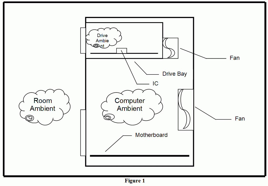 |
 |
  |
|
It represents a an IC mounted in some computer gismo like a CD ROM or hard drive. (see Fig 1). It does not take long to realize that asking the question: "The room temperature is 50 degrees, how hot does the IC get?" is nonsensical. The first problem is that we need to know how much heat is being created in the IC. This is based on three major factors:
The other factor in how hot this IC gets is the amount of heat that can be removed from it. Now things can get really messy. Start with the |
 |
  |
|
die. After all that is all that really matters. You are trying to keep it form getting to 150 degrees or whatever we recommend. Is the die epoxied to the lead frame? Then there will be a worse-case thickness for that epoxy and that will interfere with the heat removal. Is there a spec for how the part is soldered to the board? Then that must be factored in. Now you can image that the heat is finally getting out of the part and onto the copper traces in the circuit board. How thick is the board? What other components are heating it? How think is the solder mask covering (insulating) the copper? The temperature of the board is determined by all this. It is the difference in that temperature to the surrounding air, as well as the airflow over it that will determine the final temperature of the IC. The temperature of the surrounding air is also tricky. For that IC it certainly isn't the room temperature. It is the temperature and movement of the air around that circuit board that is spreading the heat out that determines how hot the IC gets. The air movement is based on a fan mounted on the back of the drive. That will also have manufacturing variations. It may also move less air as it gets dirty with use. And if the power to the fan is low it will move less air. The part could run from 5 volts and be at 5.5 max and the fan could run from 12 volts and be running at 10.8 volts minimum. Fun huh? But that air the fan is drawing past the part may come mostly from inside the computer, not form the room. So then you have to factor in the worse case computer case temperature. This is also based on how many things are installed and how hard they are running. Then there is a whole different fan that is trying to get cool air into the computer enclosure. One thing is for certain: If the room air is at 50°C the air around that IC is certain to be higher. Another fact is that if the room temperature increases by |
 |
  |
|
10 degrees the die temperature will have to increase by at least that amount. 1.5 It's all about the die temperature. The above discussion shows why no semiconductor manufacturer can say the parts will always work at any given ambient temperature. We have no idea how the customer will mount the part, use the part, power the part and cool the part. All we can quantify is the die temperature. We can say: "If you keep the die under this temperature you will get acceptable part life". It is also true for the specifications of the part. Although we include tables and charts that specify the part's operation at a given ambient temperature we also specify the load and power conditions that insure we will never expose the die to more then 150 degrees C. Just as it is nonsensical to ask what the die temperature is versus an ambient without knowing the exact system and use of the part, it is nonsensical to ask; "How good will the part perform at a certain ambient?" The only thing we can measure that is definitive and absolute is part performance over the die temperature. 1.6 Conclusion. As operational amplifiers and other analog components handle more and more power it is essential to understand and quantify the temperate of the die. It is soon obvious when a part melts but in addition to the linear relationship with part life to operating temperature there are several other failure modes. When the silicon operates over 150 degrees C and it is in contact with the epoxy used to mold the package the heat damages this epoxy. At very high temperatures, above 200°C, the epoxy just starts to melt and burn and things go downhill very rapidly. The epoxy has a glass-transition temperature of about 170°C. If the silicon gets near this the plastic degrades and begins to decompose. The |
 |
  |
products of the decomposition are conductive and can short the part out internally. In addition the decomposed matter can migrate through imperfections in the silicon's passivation layer and cause all kinds of havoc including mysterious noise problems. This study offers detailed explanations of two essential methods for die temperature calculation. One uses the internal ESD diodes used on every pin of a modern IC. The other involves using a thermal (IR) camera to view the heat of the die directly. The ESD diode method is very useful because it can be used to measure a part operating in a system. The disadvantage of the ESD diode method is that it will only tell you the temperature of the ESD diode itself. The hottest part of the die will often be the outputs. These investigations have shown 50 degree variations of temperature across a die and 25 degrees between the ESD diode and the hot-spot. This is not a universal rule however. The actual differences will depend on the process and application of the part. It is the duty of the application engineers and the engineers at the customer to fully understand and characterize the die temperatures that whey will be exposing the parts to. 2. ESD diode temp measurement2.1 Theory. Silicon diodes have a very linear and stable relationship between the forward voltage and the temperate that they are at. There is some fancy formula and it probably involves Boltzman's constant but math won't be too much help in this case. |
 |
  |
|
Although the relationship between voltage and temperature is linear the absolute value depends on four things:
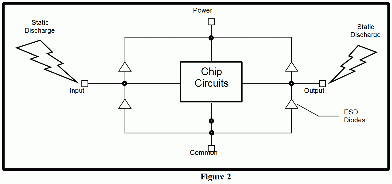 The diodes shunt current around the chip circuits and into power or common. In order to create a forward voltage across an ESD diode it is necessary to bring the pin voltage either above the power supply voltage (to bias the high-side diode) or below the common voltage (to bias the low-side diode). A pin must be available that can be dragged outside the rails during normal operation. Often there is an enable pin that can be raised above it's power rail. Other times it may be possible to find an open-collector output that can be dragged above the power supply. A knowledge of the internal circuitry is needed since dragging the pin outside the rails may forward bias a |
 |
  |
|
transistor base-collector junction or exceed the base-emitter breakdown voltage. Once the right pin is determined the ESD diode can be calibrated for its forward voltage versus temperate. The part can be put in an oven and the ambient temperature changed while measuring the ESD diode forward voltage. This must be done with a precise and known current going through the diode. Once the diode is calibrated in an over then the part can be run in the circuit while the same current is being injected to the pin. The voltage measured should be related to the ESD diode temperature. Should be but not always. Care must be taken that the power and ground paths inside the part do not have significant voltage drop due to the current they are carrying. Remember that the ESD diode voltage can only be measured between a given pin and either the power or common pin of the IC. The schematic shown in Fig 3 should make this clearer. 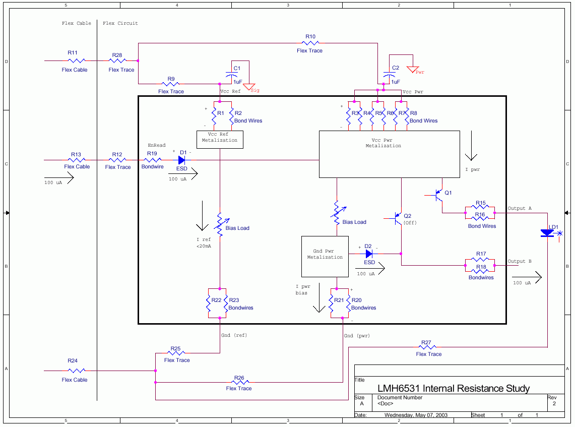 . It can be seen that if there is significant current in the Vcc Power bond wires and metalization then there will be a corresponding voltage drop. Looking at the voltage of ESD diode D1 that is connected to this Vcc plane we can see that the voltage drop due to current flow in the Vcc circuit will subtract from the ESD diode voltage and give a falsely low (hot) reading. Similarly if one was measuring ESD diode D2 |
 |
  |
|
any current flowing out of the ground pin will also create a voltage drop. This will also subtract from the ESD diode voltage and create a false low or hot reading. If one makes the uncertain assumption that the ESD diodes are at the same temperature it is possible to calculate the internal difference due to voltage drop and estimate the internal resistance of the bond wires and metalization. This can be used to correct the ESD diode voltage. There are also techniques being examined to apply the current suddenly and not the voltage drop due to this current before the ESD diode changes temperature. In addition it should be possible to measure the internal resistance directly on a probe station. 2.2 Practice. This section outlines the real measurement of ESD diode temperate and points out some of the pitfalls you may encounter. Although the theory sounds relatively simple there are several caveats that need to be paid attention to in order to get good results. The following mistakes are possible.
The first issue is relatively simple to resolve. A calibration run had been made where an ESD diode voltage was appreciably lower (hotter) then any of the other ESD diodes measured on the part. The low reading diode was on an |
 |
  |
|
enable pin. The error in this case was that the diode was characterized with power applied to the part. When the Enable pin was raised high the part turned on and a significant amount of quiescent current began to flow (over 100 mA). This current heated the part above the oven temperature. It is a handy trick to remember that the part need not be powered or turned on in order to measure the diode temperature. Just two wires are needed across the diode. It is best if the part or board is in an oven as opposed to being under an "elephant" as the entire board is assured to be isothermal after a few minutes at a given oven temperature. 2.2.2 The oven set point temperature may be inaccurate The second issue is also simple to resolve. An external in-calibration temperature measurement system can be used to insure the data recorded is accurate. It is not necessary to take the data points at even numbers such as 130 degrees. All that matters is that the diode forward voltage is recorded with the actual temperature--Say 132.4 degrees and 0.869 volts. 2.2.3 The diode currents may be different There can be major confusion if the forward current being stuffed through the diode is different for different runs. In this case we made some tests at 100uA diode forward current. Then, fearing that the diodes were self-heating due to this level of current, a value of 20uA was used. Even though both are valid when comparing the oven calibrated data to the operating data it can be easy to apply the voltage measurements at one current to the calibration data taken at a different current. The fears of diode self-heating were unfounded and 100uA was determined to be a practical value, low enough to avoid self-heating and high enough to swamp out any leakage currents. |
 |
  |
|
2.2.4 There may be external circuitry on the board that distorts the measurement. You must insure that if the part is mounted on a circuit board there is no other components that will rob or add current from the diode. In one case an input pin had a 50 ohm termination that effected the measurement. One could argue that it will all be calibrated out but if you are claiming to measure ESD diode voltage over temperature in an oven that is what you should do, not measure an ESD diode in parallel with a 50 Ohm resistor. Of course, even more important os that the parts is removed for both the calibration in the oven and when the board is being used and the temperature is being measured. 2.2.5 There may be internal circuitry in the part that distorts the measurement. One must be careful which pin is picked and also whether that pin is pulled above or below the rails. It will be necessary to consult with the IC designer or have a set of IC schematics handy. In general you must avoid forward biasing any base-collector junctions. It may be possible to cheat this rule if the forward biased junction is near the ESD diode. If they remain isothermal to each other then the measurement will be accurate. It the transistor is in the middle of the die and it gets hot while the ESD diode is cooler then the measurement will not be valid. 2.2.6 The test equipment may induce errors. The voltmeter used to measure the forward diode voltage should have a very high impedance. Some voltmeters auto range this impedance. The HP meter I used had to be set to have a 10Gohm input impedance. This insures that none of the 100uA forcing current goes into the meter. There is also some concern about the use of the Keithley current source. We have tried to measure the instantaneous |
 |
  |
|
voltage drop across the diode with a scope when the power is applied suddenly. The current source may not respond this sudden change and may have stray capacitance effects. It may be better to use a high value resistor pulled up to a high (~30 Volts) in order to inject the 100 uA. This will have less stray capacitance and inductance and may provide a cleaner signal. 2.2.7 There may be power or common currents that distort the measurement. This is a critical issue. Initial measurements showed the ESD diode was at 170 degrees C. After realizing the internal currents were artificially lowering the ESD diode readings it was apparent that those measurements were off by 50 degrees. Furthermore if the ESD diode voltage is measured far away from the actual IC pin there may be further voltage drops in circuit board traces and cable runs. 2.3 Procedure. Based on the lessons learned in the above discussion the following is a procedure that has been developed for one part, a laser diver IC. It should be remembered that this procedure only applies to this particular chip. It is an example only. You have to understand the principles involved to get a valid measurement for a different IC. 2.3.1 Pick the pin(s). The first issue with this part was to pick the proper pin to measure. Initially the Enable pin was chosen. It was decided to raise this pin above the rail to forward bias the high-side ESD diode. This pin was chosen for several reasons. The pin is always high when the IC is being used so strapping this pin high by injecting 100 uA into would not interfere with the operation of the chip. In the customer's circuit this line had no other components on it and was convenient to reach. |
 |
  |
|
The ESD diode measures was reasonably close to the transistor output array so it would be at a close temperature to this hot spot. Unfortunately this pin goes to an internal structure show in figure 4. 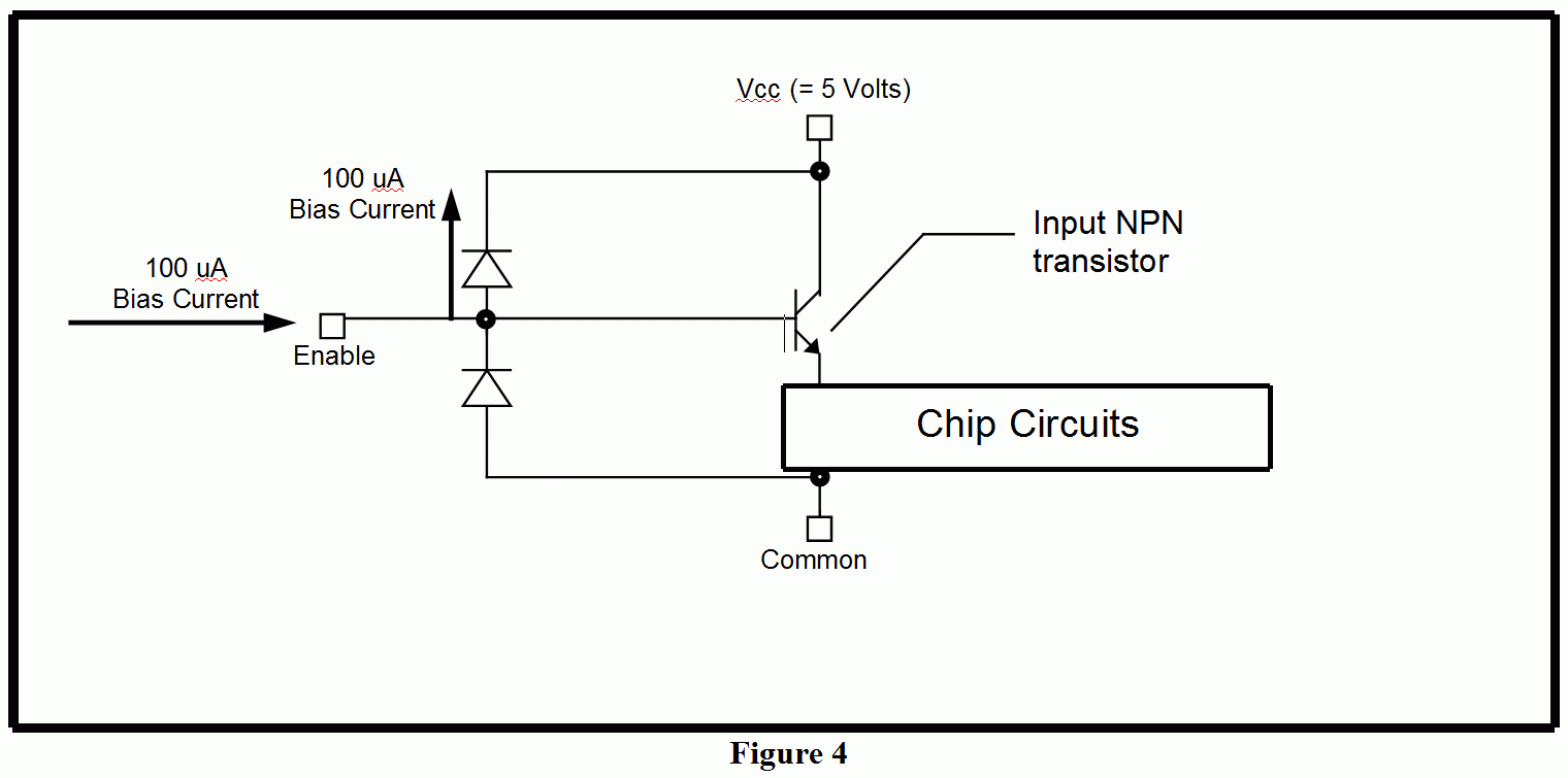 . It can be seen there will be a tiny current into the base of the transistor but in view of the circuit that is was attached to those currents are negligible. The real problem is that NPN transistor itself. If that enable pin is raised to 0.7 volts above the Vcc line the NPN transistor will have it's collector-base P-N junction forward biased and some current will flow in this junctions as well as in the ESD diode. This will calibrate out if the transistor and the ESD diode are at about the same temperature but if the two junctions are calibrated isothermally (because they are in an oven with no power to the chip) and then they are at different temperatures on the chip (because the transistor may be closer or farther away form the hot spot) then this will cause an error. It turned out that the transistor was very near and rather isothermal to the ESD diode but it was decided to use a different pin. There was a brief effort to use the Enable Oscillator pin pulled low since that ESD diode is very close to the output array and it was felt would give a very accurate temperature. It turned out to be a bad choice because this pin has a PNP transistor input and pulling it below the rail forward biases the collector-base junction of that transistor. Furthermore the ESD diode and the transistor are far apart on the die and the error to |
 |
  |
|
differential heating was very pronounced, unlike the Enable pin. After consultation with the IC designer (you may want to do this first and save all the drama) it was determined that raising the Enable Read pin high was a good pin selection. The pin has to be enabled at all times when the part is working, there are no NPN transistors connected to it to get forward biased and the ESD diode was fairly close to the output array. Later it was determined that there were significant currents in the Vcc bond wires and metalization that caused this measurement to be in error. Therefore it was necessary to pick a pin that could also be measured that did not have the Vcc currents flowing in one side of the ED diode. It was decided to use the Output B pin (while using output A). By bringing this pin below ground it is possible to measure the low-side ESD diode. Referring to figure 3 you can see why this choice was made. It was also important that this ESD diode was abut the same distance from the output transistor array because the correction factor calculated assumes that the two diodes are at the same temperature. 2.3.2 Prepare the board. The Read Enable pin had a 50 ohm termination resistor and the output B pin had a 10 ohm load resistor. Both these were removed. In the figure below 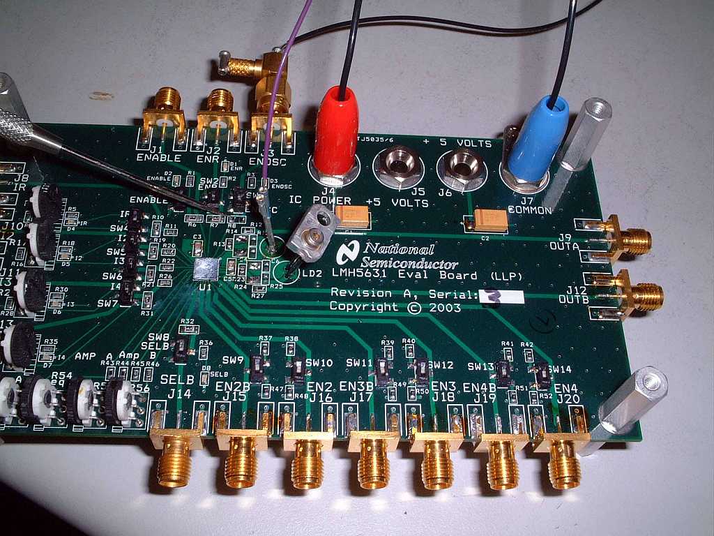 you see the wires attached to you see the wires attached to |
 |
  |
|
power and ground as well as soldered to the Output A pin that was being measured for this run. This was later changed to Output B. This run was calibrating the EnOSC pin. This was later changed and a new run was made with the Enable read pin next to it. The scribe pints to where the 50 ohm termination resistor was removed. You may also note the 10 ohm load resistor is not soldered into the output line. There is an actual laser diode soldered into the output B circuit during this run.
2.3.3 Calibrate the ESD diodes in an oven. This can be done with an "elephant" temperature system but an oven is preferred because the entire board is assured to be isothermal. 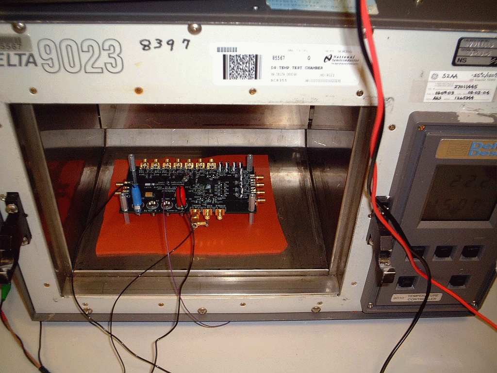 Because we were measuring two ESD diodes, four wires were needed to be run from the test board. The pins enable read and output B needed wires run and both power and ground had to be brought out. When measuring the high-side ESD diode on the Enable Read pin the 100 uA was pushed into the Enable read pin which raised it about 0.7 volts above the Vcc pin. When measuring the low side Output B ESD diode the current was sent into the common (=ground) pin and taken out the Output B pin. This forced the Output B pin about 0.7 volts below the Ground pin. Figure 6 shows the board in an oven. A rubber pad was |
 |
  |
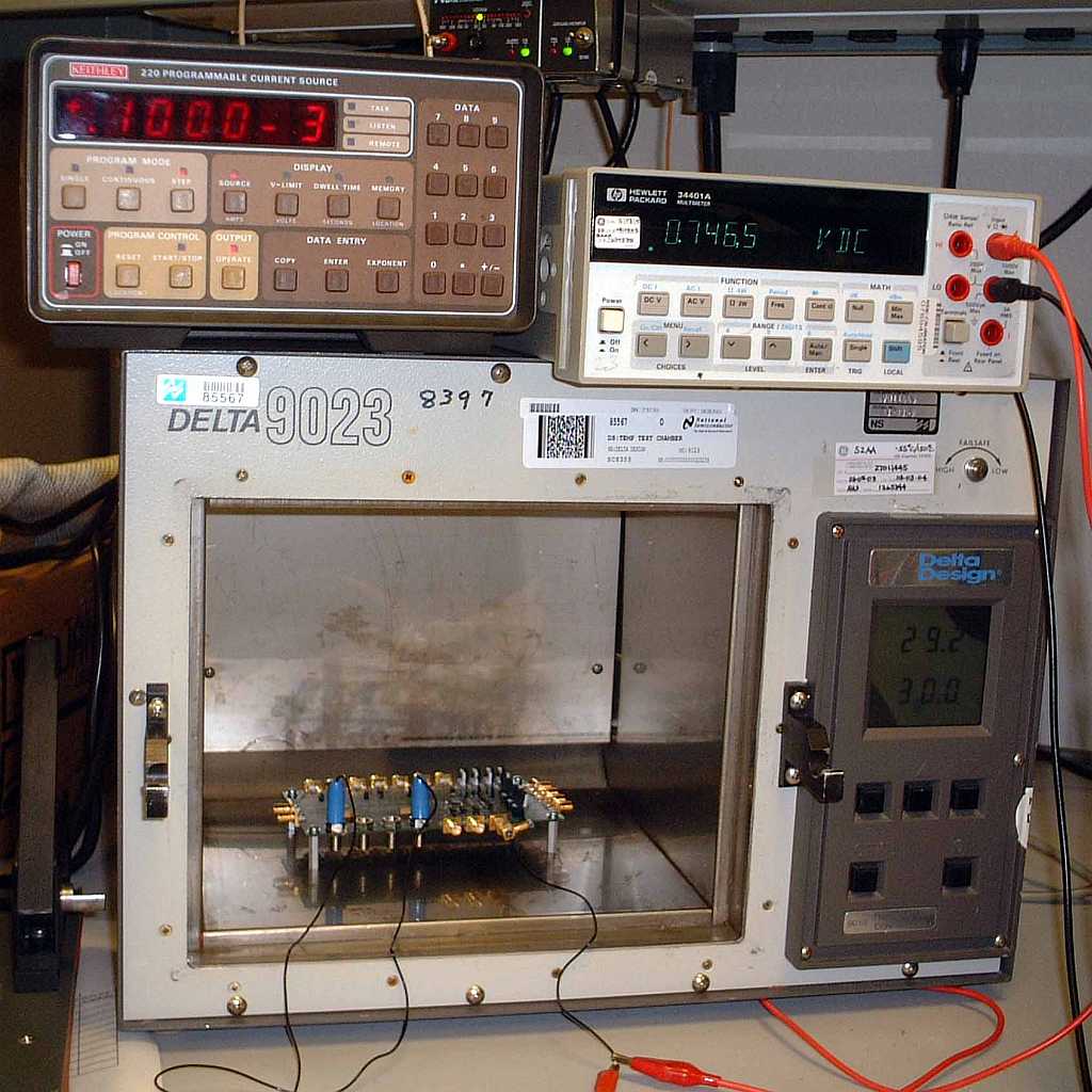 placed on the bottom of the oven to insure there were no ground currents or other leakage currents between the diodes and the test equipment. 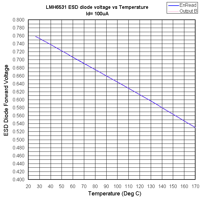 Not show in the picture was a separate temperature measurement device used to insure that any error in the oven set point would not corrupt the data. After the oven was run to several temperatures and the board was allowed to soak for a few minutes the diode voltages |
 |
  |
|
became stable. The temperature and voltage was recorded and this data was entered in a spreadsheet. A plot was made which is reproduced below. It should be noted that there are two lines on this chart, one for the Enable read ESD high-side diode and one for the Output B low side diode. The forward voltages were so close in value that the lines are right on top of one another over the entire range of temperatures. This gives reassurance that the data is valid. 2.3.4 Determine the internal resistance correction factor. After noticing that the implied temperatures of as measured by the ENREAD pin were far too high it was realized that there were internal resistances inside the chips Vcc circuit that artificially lowered the measured ESD diode voltage. This can be ascertained by referring once again to figure 3. In order to get correct temperatures from the ESD diode it is necessary to estimate this internal resistance. Then it is necessary to measure the both the diode voltage and the current into the Vcc pin to calculate the actual ESD diode temperature. There are four methods to estimate the internal resistance:
|
 |
  |
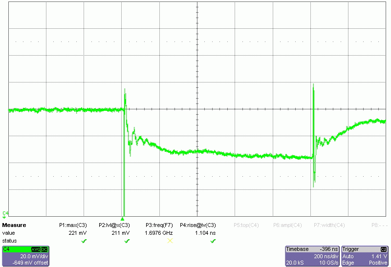 The right image has a soft turn on because it it's the global chip enable that is being toggled 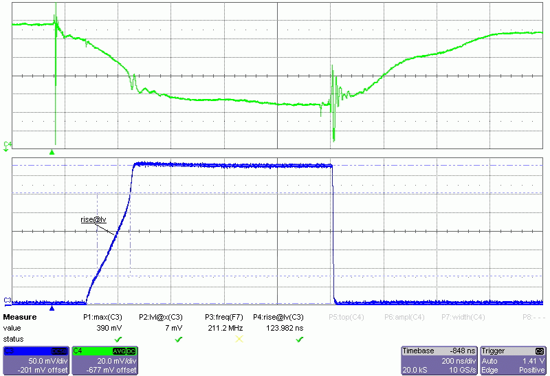 as as |
 |
  |
|
opposed to the left image that has the chip already running but the write pulse is being toggled on and off. It is the trailing event that is most informative in both images. Note that voltage level seems to jump up about a half a division in both cases. The right hand image shows the thermal changes very well after the trailing event.Notice that the three different slopes of this signal imply at least three thermal time constants in the device. Using another ESD diode to calibrate the primary one requires a secondary diode is available and that that diode is the same temperature as the primary ESD diode. Measuring the part on a probe station can be difficult since the topology also effects the diode voltage relative to the series IR drop. For this particular part is was decided to evaluate the Output B ESD diode at the same time as the Enable Oscillator ESD diode. The Output B diode is a little further away for the transistor array so it's higher reading may be due to a cooler temperature, not the IR drop in the Enable Read ESD circuit. There is also an appreciable current flowing in the Ground pin metalization, which inspection of figure 3 will show, will also artificially depress the measured number and once again make the estimated diode temperature too high. Since this errs on the side of conservative measurement it was felt this is an acceptable method until others can be perfected. It should be pointed out that the Output B diode was not chosen as the primary diode because there is a Laser diode connected to the output in a real application and it would be more difficult to evaluate this pin compared to an input pin. Putting a current of 200 mA into the part the two ESD diodes had a difference of 44.6 millivolts. If the diodes are isothermal and there is no current in the ground pin then the difference must be due to the IR drop in the Vcc plane that artificially lowers the apparent reading of the Read Enable ESD |
 |
  |
|
diode. The 44.6 millivolts divided by the 0.2 amps yields a Vcc plane resistance of 0.22 ohms. By adjusting the chip bias so that there is 400 milliamps flowing into the power pin then the diode readings were different by 84.1 millivolts. Diving this by 0.4 amps implies an Vcc plane resistance of 0.21 ohms. The correlation of these numbers is comforting but it must be kept in mind the basis of the calculation is on an assumption of the two ESD diodes being isothermal and that there is no current flowing in the ND pin. For now the correction based on 0.21 ohms Vcc plane resistance is considered adequate. The implications of this correction may be thought of as such: Whatever voltage is measured on the Read Enable ESD diode is known to be too low because of the IR drop in the part. The real ESD diode voltage is given by multiplying the input current by 0.21 ohms and then adding that resultant voltage to the ESD diode voltage. For instance, if the Read Enable ESD diode measures 0.500 volts and the part is drawing 450 milliamperes, you take the 0.21 ohm internal resistance times the 0.450 ampere current to get 0.0945 volts. That means the real Read Enable ESD diode temperature is 0.500 plus the 0.0945 correction factor to get 0.594 volts. Since we can see the slope of the ESD diode voltage is 1.6 millivolts per degree C you can see the 94 millivolt correction represents a temperature correction of 59 degrees. Once it is understood that the input current must be factored into the ESD diode measurement it is easy to set up a spreadsheet to correct the measured values. 2.3.5 Use the corrected ESD diode voltage to calculate temperature Having a valid ESD diode voltage allows the temperature to be calculated directly. Since the variation of diode temperature with voltage is a straight line the math is rather easy to determine the temperature. Since the temperature follows |
 |
  |
|
the simple "y = sx + a" form, The value of any temperature on the X axis of the chart in figure 8 is given by x= (y - offset @ zero degrees) / slope where x is the temperature in degrees C, y is the ESD diode voltage, the offset @ zero is the ESD diode voltage at zero degrees. Remember that the slope of an ESD diode is negative. Since this experiment did not calibrate the diodes all the way down to zero degrees the number can be interpolated by taking the a given temperature such as 26 degrees and multiplying by the slope of 1.6 mV/degree. The add this to the diode voltage taken at the 26 degree temperature. For example, the oven-calibrated ESD diode voltage is 0.7587 volts at 26.6 degrees. The slope of the calibration run is 1.5907 millivolts per degree C. So go back the 26.6 volts to zero degrees by multiplying by the slope ( in volts, not millivolts) to give a value of 0.04231 volts. Add this to the voltage at 26.6 to get 0.8010 Volts at a diode temperate of 0 degrees. Then you can set up a spread sheet that takes any given diode voltage, subtracts 0.8001 volts and then divides the result by -0.0015907 volts/Deg to give the temperature. The results can be plotted in a chart or used as the x axis of a chart where temperature is the forcing function variable. 3. Thermal Camera temperature measurement3.1 Theory.It has been long known that silicon phototransistors are very sensitive to infrared energy. Since both CCD images and CMOS imagers are using the phototransistor effect they too are sensitive to infrared (and hence, thermal) images. Conventional cameras actually filter out the IR light and make other adjustments to provide a proper output for various wavelengths of light. An infrared camera filters out the visible light and it's optics |
 |
  |
|
are made to pass the infrared image to the CCD imager. There are two camera's known at National. One is an expensive FLIR thermal camera owned by the packaging group that is currently inoperative and apparently un-fixable. The Display Group has a less expensive but quite adequate Compix thermal camera. The theory is quite simple. Deceptively so, especially if you trust software. You point the camera at the die, click on the "Scan" button and admire the pretty picture. The software can display the infrared energy as a black and white image or as a color map with reds and white being hot and blues and black being cold. The color map image is generally most useful for quantifying temperature gradients. 3.2 Practice. As always, the practice of thermal imaging is far more complicated. The issues that arise generally fall into three areas.
The first issue that will effect the accuracy of the thermal image is the emissivity of the hot surface, the die in this case. A shiny surface has a low emissivity--it will radiate less IR energy then a dull surface. A dull black surface has an emissivity of 1.0. This is the default emissivity used by the software. It may be possible to characterize the emissivity of a silicon chip but it would be difficult. A fundamental problem is that the emissivity is very likely different from the areas of the die that are metalized versus areas that are not. For this reason it is far simpler to just coat the die with film with a known, good emissivity. Flat black spray paint is ideal for this. |
 |
  |
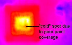 It's emissivity is 1.0 and there is enough resin in the paint so that it is relatively non-conductive. Figure 9 shows a thermal image of a die that has a dark "cold" spot on it. Investigations showed that this was due to poor paint coverage on the die, the dark spot had poor coverage and the shiny die metalization was showing. 3.2.2 The focusing of the camera. The second issue to deal with is focusing the image. Since the camera is not operating real-time (it takes about 20 seconds to make a scan) it can be quite time consuming to get an acceptable image. A key help is to put the software in a mode to display black and white images. This makes it a little more easy to interpret the picture. 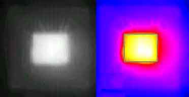 Figure 10 shows the difference between a black and white and color image. This display is controlled in the software under the "Display/colormap" menu. It can be very tedious making minor adjustments in the focus |
 |
  |
|
of the camera and then scanning and reviewing the image but this must be done to get good data. 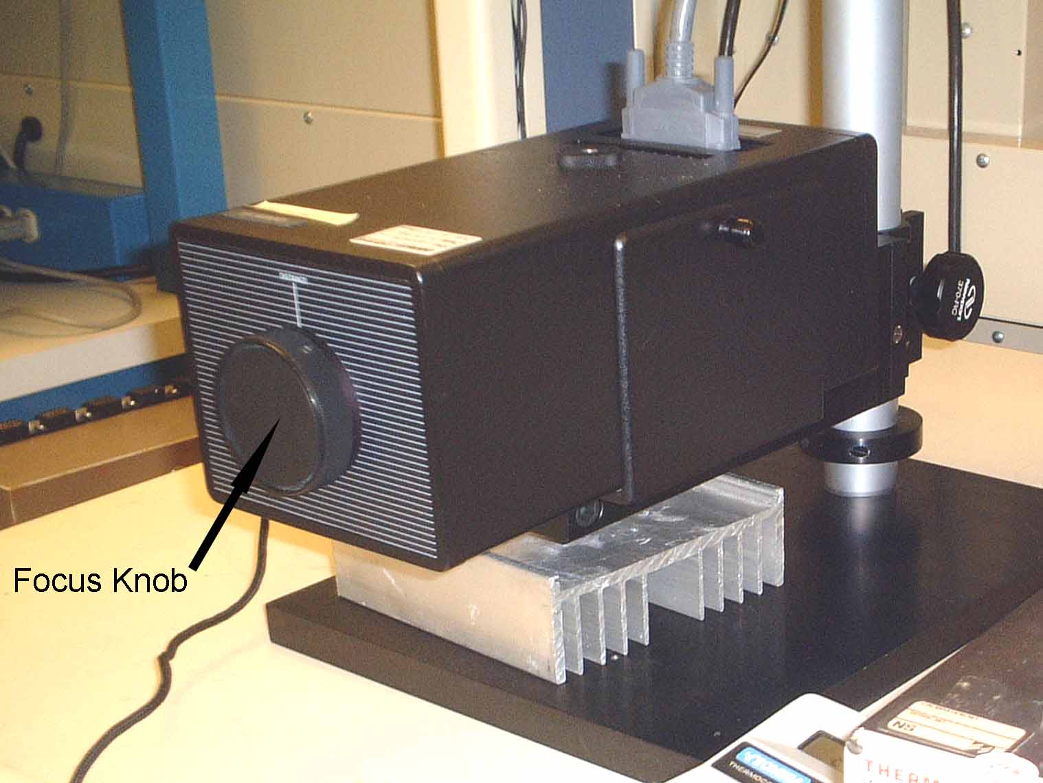 Figure 11 shows the camera and it's focusing knob. In order to get good results there must be a lot of contrast in the image. This is done by having an image with steep thermal gradients. In other words, it is easier to focus a part that is very hot rather then a part that is all at room temperature. Once the focus is found the part can be operated in various regimes to show the cooler operating temperatures. A good indicator of the focus quality is the appearance of distinct bond wires as in the black and white image above. 3.2.3 The software parameters that effect the measurement. As in most software, it is very easy to have software settings that will give poor results. |
 |
  |
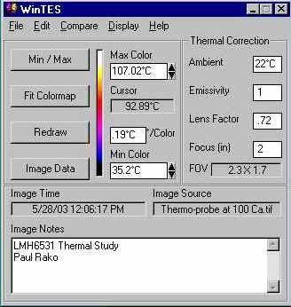 Figure 12 shows the software control dialog. The "Thermal Correction" area has four settable parameters that can radically effect the measurement. 3.2.3.1 Ambient Temperature The ambient temperature defaults to 21 degrees C. This is usually close enough to provide good results. If you want to provide better results, then measure the room temperature and enter it into this box. 3.2.3.2 Emissivity This parameter can account for the varying surface textures and colors of the part being imaged. Since we paint the die a flat black this can be left at the default value of 1. 3.2.3.3 Lens Factor This is a correction factor that allows for the differences in various lenses. Since this camera has the 7-power lens installed the default of 1 has to be changed to 0.72. |
 |
  |
|
3.2.3.4 Focus (in) This parameter can cause huge measurement errors. This was first noted when the ESD diode temperature data was very different with the thermal image data. The camera defaults at 10. Although one would think that the 7X lens might change this to 1.4 inches a calibration run noted below established that a figure of 2 provided images that were best matched to the ESD diode temperatures that were being measured at the exact same time. Note that the Focus ring (which is labeled "distance" on the camera) has distance numbers on the barrel in millimeters. Dividing this setting by 7 and converting to inches to account for the lens did not provide for the most accurate correlation between the ESD diode temperatures and the thermal image temperatures. Bear in mind that the "2" entered was for a specific focus distance used in the run. The best number to use will depend on the actual focus distance used. 3.2.4 A calibration method. In order to verify that the software parameters above were set at a reasonable level a calibration procedure was used to evaluate the accuracy of the camera. A heated thermal probe was used to compare the thermal image data to the actual probe temperature. This instrument is shown in figure 13. 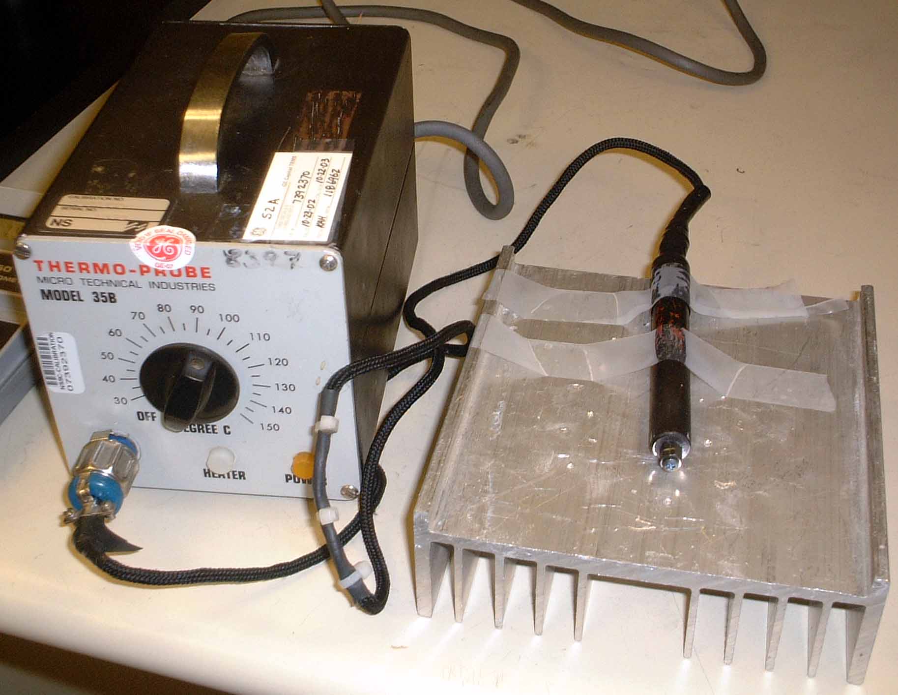 |
 |
  |
|
The knob on the box can set the probe temperature anywhere for 30 to 150 degrees C. These temperatures were verified with a thermocouple instrument. The black probe tip has been taped down to a heat sink purely to stabilize it during imaging. A small standoff was mounted to the probe tip with a 4-40 screw and this standoff was painted flat black with the same paint used to paint the die surface. 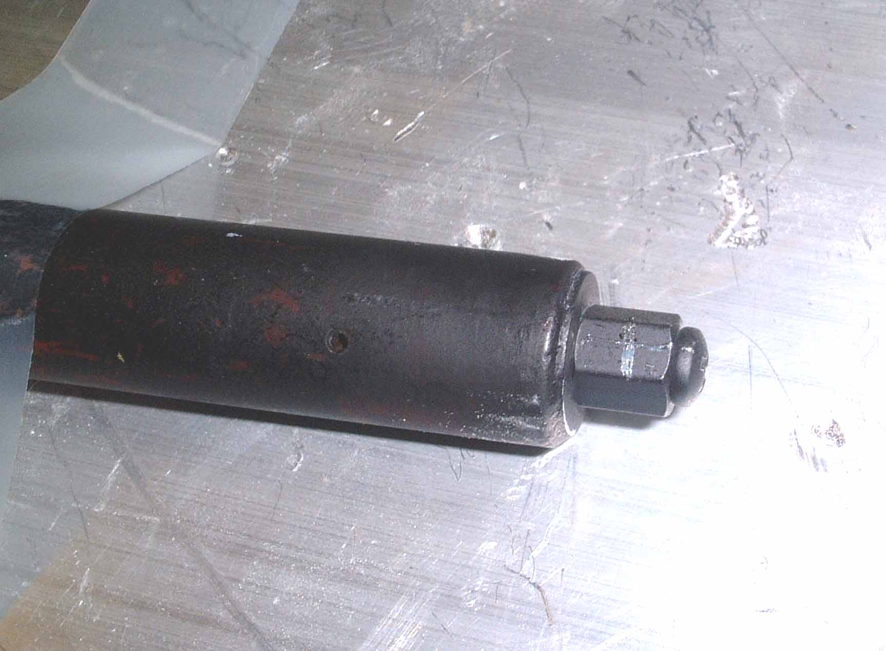 A close-up of the tip can be seen in figure 14. After an inordinate mount of time was spent trying to focus this probe tip in the camera a small cross was scratched into the paint on the standoff to reveal the bright metal surface underneath. These scratches are visible in the picture. The addition of these scratches made focusing far easier. 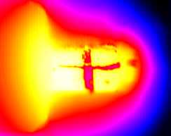 |
 |
  |
|
Focusing was done with the tip set to 150 degrees to provide the highest contrast for focusing the image. An image of the color thermal map produced by this probe tip is in figure 15. The probe temperature is correlated to the hottest part of the image which corresponds to the base of the standoff where it mounts against the probe tip face. 3.3 Procedure. Based on the practice developed above a procedure to make a thermal image is as follows: 3.3.1 De-cap the parts and mount on the board. The dapping lab is in the west side of the lowest floor in building D. It is near the library. There is a cubicle with forms and a place to drop off the forms and the parts you want de-capped. In general it is very difficult to de-cap parts mounted to circuit board unless there are no other components 4 inches around the part you need de-capped. Since these were LLP parts it was necessary to mount the parts to a board using a Metcal reflow workstation. One problem is that the Metcal has to pick up and place the part by using a vacuum tip on the top of the part. Unfortunately there is no top of the part and the die is too small for the Metcal tip to operate on. 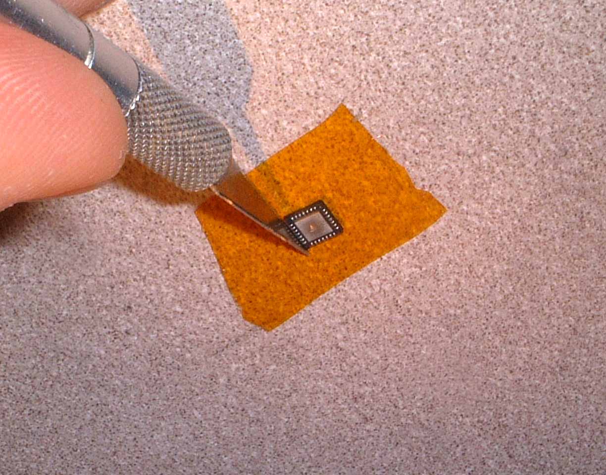 |
 |
  |
|
This is solved by placing some high temperature kapton tape on the top of the part so that the Metcal can pick up and place (or remove) the part. Figure xx shows the part being stuck top-down on the sticky side of the kapton tape. An Exacto knife is being used to trim the excess tape from the periphery of the part. 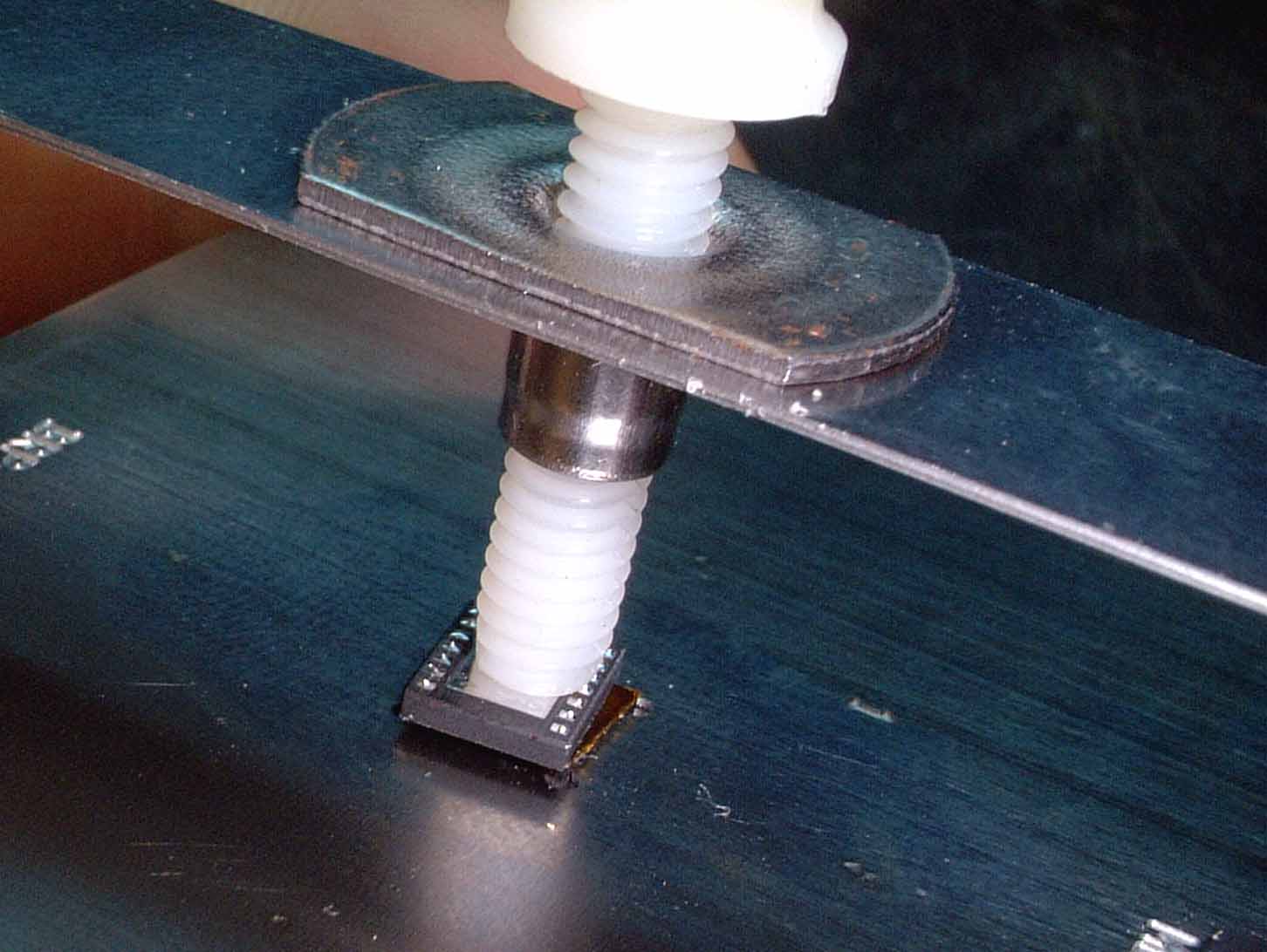 The next figure show a method to deal with a related problem. The Metcal clamps the part into the stencil for the application of the solder past. The Kapton tape is not strong enough to withstand the force. A simple fix is shown where a spare part is used to bridge across the open well covered by the kapton tape. There were attempts made to apply solder paste while simply holding the part delicately in the stencil but this was clumsy and allowed paste to creep past the stencil outline. 3.3.2 Paint the chip die flat black. 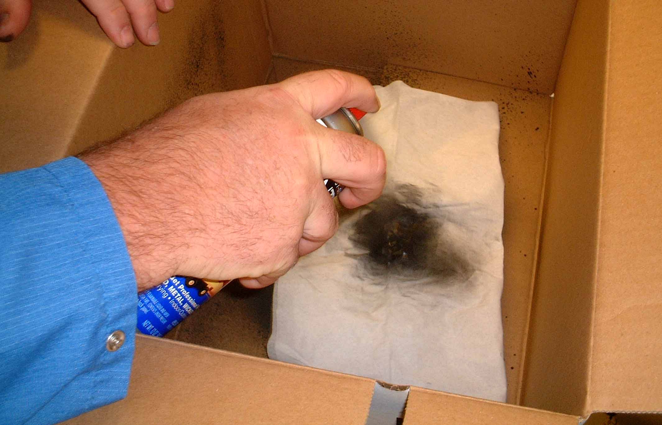 |
 |
  |
|
A small mask can be made from paper or masking tape can be used to keep the flat black spray paint off the circuit board. 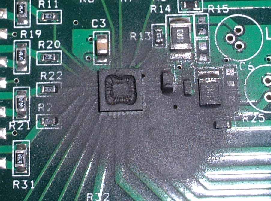 Care should be used to get a thin uniform coating that has no die surface showing through. You did take the kapton tape off right? The figures speak for themselves. 3.3.3 Place the board under the camera and focus. The camera should be lowered as close as possible to the board. This increases the apparent size of the IC. 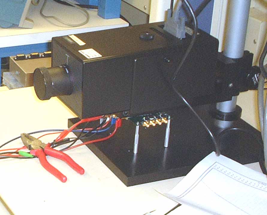 It is possible to be a few inches away if you want to see two ICs or for some other reason. Without the 7X lens the camera can be used to evaluate thermals on an entire circuit board and the distance can be 20 inches or more. |
 |
  |
|
As mentioned before the focusing is best done with the part very hot but once the focus distance is set the board can be removed and replaced as long as it is exactly the same distance from the lens. The figure shows the board under the camera. 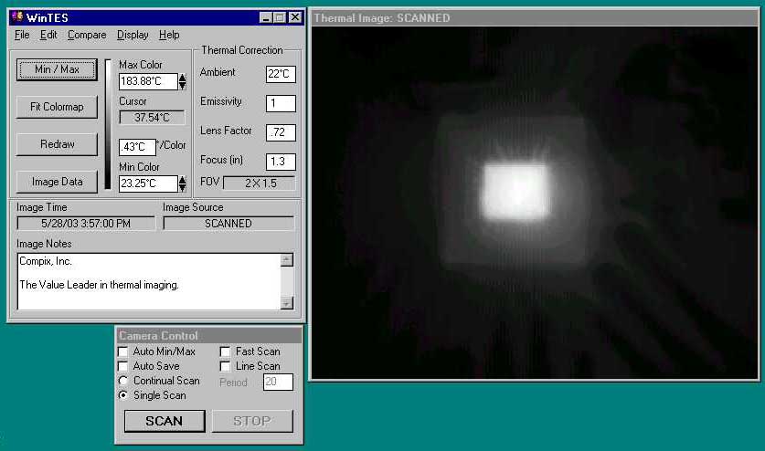 The next picture shows the chip with the colormap set to Black and White. This can be changed back and forth between color and black and white at will once the scan is taken, the colormap is just a software artifice used to represent the data. Notice that the bondwires can be seen once the focus is set. Also notice how hot the part is being run in order to get a good high contrast scan that is easier to focus. 3.3.4 Enter the proper correction factors in the software. For this run the ambient temperature was measured as 22 degrees, the emissivity remained at 1 and the lens correction factor was 0.72. 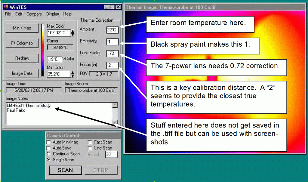 The focus distance was set to 2 inches based on |
 |
  |
|
the calibration runs comparing the ESD diode temperature and the image temperature on the die where the particular ESD diode was located. This next screenshot shows the other functionality for the program. 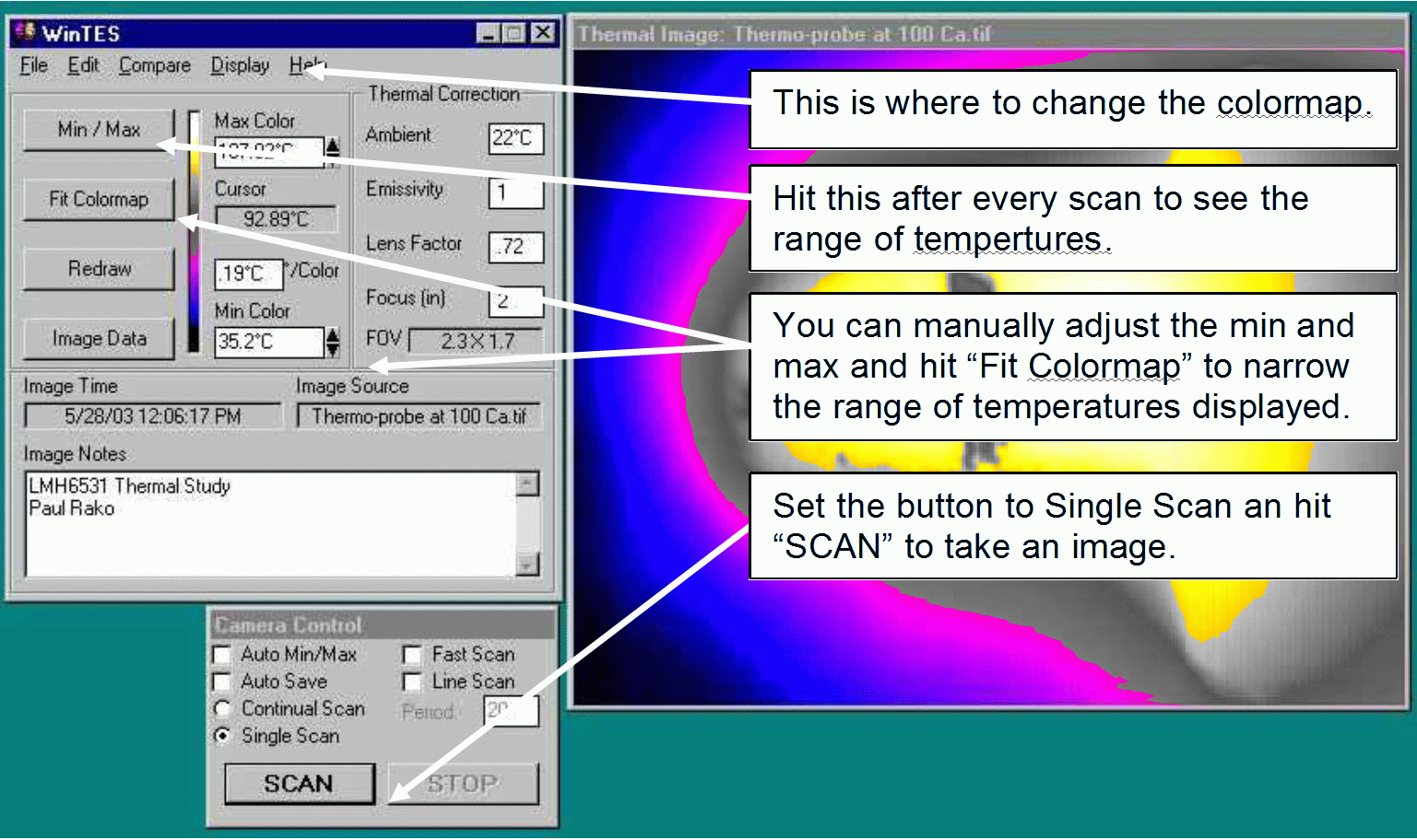 . 3.3.5 Take the scan and adjust the colormap. After clicking on the "SCAN" button the camera will have taken the image in about 20 seconds. The first thing to do after taking the scan is to click the "Min/Max button to fit the full range of scanned temperatures to the colormap. Once this is known you can draws a rectangle over a certain area with the cursor. The software will display the statistics for this area.  In addition to drawing the rectangle you can simply position the cursor over the image and the temperature at that point will appear in the "Cursor" box in the control software. This will allow the setting of the Min Color box to allow a tighter range of temperatures to be displayed. |
 |
  |
|
In the next image the value of "145" was typed into the "Min Color" dialog box and the "Fit Colormap" button was clicked. This shows the range of temperatures between 145 and 185 displayed on the die itself.  The picture has been zoomed way in and you can make out the individual pixels that the camera scanned. Since manipulating the colormap does not move or change any of the original scan you can combine the results of these two scans in a program like Photoshop. By importing the Tiff image of the entire color range it is often easier to determine where the edge of the die is. A box can be drawn around the die in this view. The box must be drawn on a separate layer in Photoshop. The expanded colormap image such as above can also be placed on a third layer in Photoshop. By arranging the layer order (outline box first) it is possible to turn off the full range image that allowed you draw a rectangle around the die and then turn on the layer with the expanded colormap of the die are only. This helps locate the edge of the die on this image and allows a better estimate of temperatures across the die. |
 |
  |
 First the full range colormap is shown on the far left. You can make out the bondwires and the outline of the plastic IC. The next panel shows a rectangle drawn around the actual die area.  The third panel is the colormap of the exact same scan but at a reduced range--the "Min Color" value was raised and "Fit Colormap" was clicked. The 1st panel shows the rectangle of the die edge superimposed over the narrow range colormap. It should be noted that the thermal images being manipulated are tiff files saved by the camera application, not screen shots of the computer. 4. Conclusions and Recommendations4.1 It is possible to measure ESD diode temperature as a part operates.The ESD diode temperature measurement method can be a very effective way to get a temperature on the edge of the die while the circuit is running. It must be remembered that the hot-spot of the die will be certain to be higher then what the ESD diode reads. |
 |
  |
|
4.2 There are significant thermal gradients across the die. The images in this presentation show gradients of over 50 degrees across the die. The die is not isothermal, especially with a dielectrically isolated process and with large power levels. 4.3 Further investigations are needed There are still unresolved questions with both methods. The ESD diode technique needs to be have an improved method of determining the correction factor. The thermal imaging needs a better and more precise method of correlating the image with real temperature data. 5. Action Plan5.1 ESD Diode Method.5.1.1 Investigate the instantaneous change method of calculating IR drop. There needs to be definitive data showing the instantaneous change correlating to the actual current change, unlike the data taken so far. 5.1.2 Measure the bondwires and Vcc plane resistance directly. This will require the chip be measured in a probe station. 5.1.3 Investigate CAD/SPICE methods to determine sheet resistivity. The resistivity in the Vcc and Gnd planes can be determined mathematically. It may be necessary to use CAD to model the unusual shape of the metalization and the point where the ESD diode ties into this metalization. 5.2 Thermal camera method. 5.2.1 Create a calibration circuit. A board will be laid out with 6 de-capped LM35 temperature sensors. The temperature sensors will be heated by resistors. The LM35 die can be painted flat black with the exact same paint used for the IC to be measured. |
 |
  |
|
Then, camera parameters can be modified until the accuracy of the image is assured. The IC to be measured can then be put under the camera at the same focal length. It may also be possible to make a little board that lays next to the IC to be measures and will serve as a calibration reference for every scan. 5.2.2 Investigate high resolution imagers. It would be beneficial to have higher resolution images available. This would allow the estimation of temperature around the ESD diode are to be more confident, among other benefits. 5.2.3 Investigate stronger lenses. The 7X lens gets a fairly good image of the die but it would be nice to get more die area in the image. The heat flowing out of the PC traces is also instructive but the surface of the die is the area of most interest.  . files |
 |
  |
This post is in these categories:This post has these tags:
|  |
  |